










Technical Resources
How KJLC's ALD Systems are Powering Next Gen Research
In-depth technical posts covering ALD process fundamentals, film chemistry, system configurations, and real-world application examples.
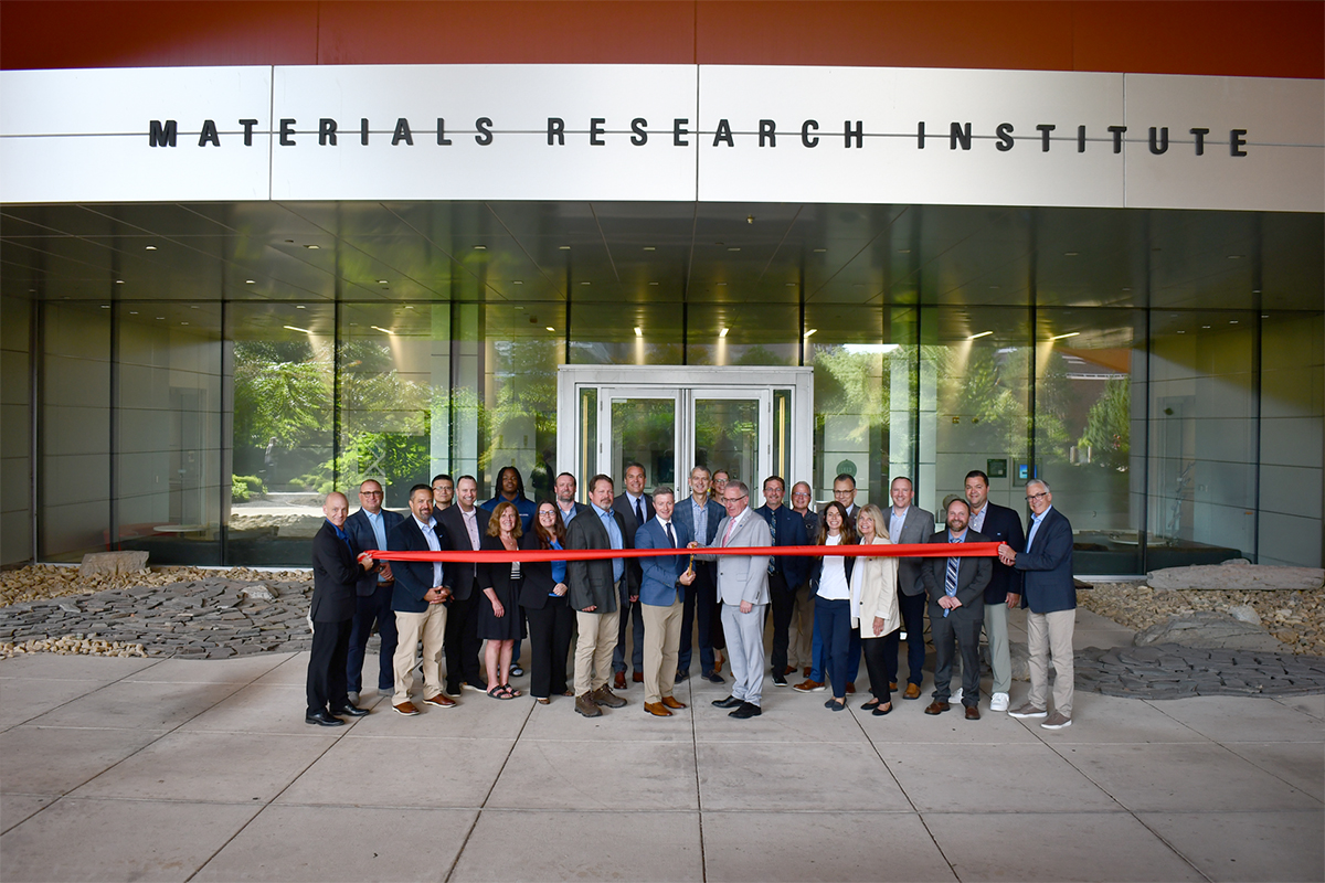
The Kurt J. Lesker Company and Penn State University have launched the Kurt J. Lesker Company Atomic Scale Processing Center of Excellence (ASPIRE), housed in Penn State's Nanofabrication Laboratory at the Millennium Science Complex...
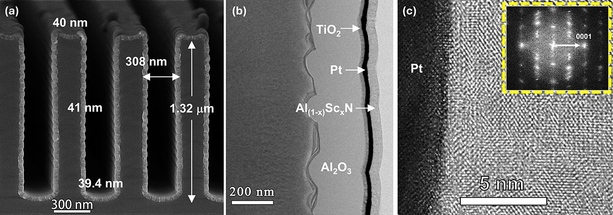
From high-purity thin films to functional ferroelectrics in 3D architectures. As semiconductor devices continue to evolve toward atomic-scale dimensions and complex 3D architectures, the requirements placed on materials are becoming increasingly stringent. Thin films must not only be conformal and uniform—they must also deliver functional properties at the atomic level, with impurity concentrations reduced to near-zero...
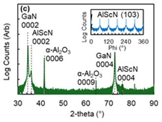
Atomic Layer Deposition of High Purity AlScN Thin Films Achieved Through Ultrahigh Purity Conditions
As semiconductor and microelectronic devices evolve, requiring atomic-scale manufacturing precision, the purity constraints on materials become extreme. At the 2nm node in semiconductor development, line widths are on the order of 40 atoms! Among the more interesting materials is the ferroelectric material aluminum scandium nitride (AlScN), a wurtzite-structured, solid solution material that combines the superior piezoelectric properties of AlN with the ferroelectric behavior introduced through scandium doping. AlScN has demonstrated breakthrough potential for nonvolatile memory, energy harvesting, microelectromechanical systems (MEMS), Rf filters, and optical devices. All of the applications require conformal, ultra-pure thin films with atomic-level precision...
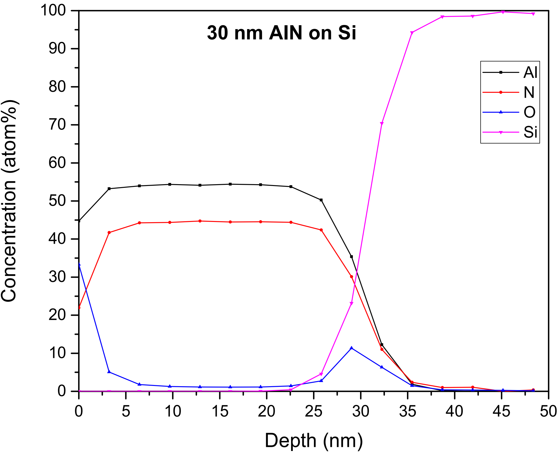
Jeffrey R. Shallenberger of the Materials Research Institute at Penn State University has led a groundbreaking study demonstrating the detection of trace oxygen levels—down to 0.1 atomic percent—in highly reactive thin films using X-ray Photoelectron Spectroscopy (XPS). This work sets a new benchmark for precision in surface analysis and thin film quality control...
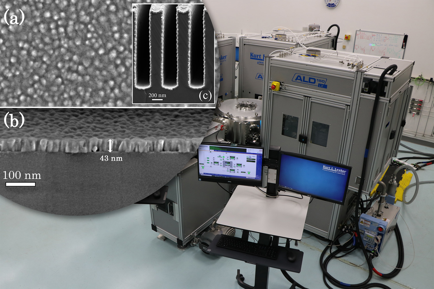
In the ever-evolving world of semiconductor technology, innovation is the key to staying ahead. At Kurt J. Lesker Company, we are proud to announce a groundbreaking achievement that promises to revolutionize the field of Atomic Layer Deposition (ALD). Our latest publication, featuring the patented Precursor Focusing Technique (PFT) and Ultra-High Purity (UHP) process capability, marks a significant milestone in our commitment to advancing next-generation applications...
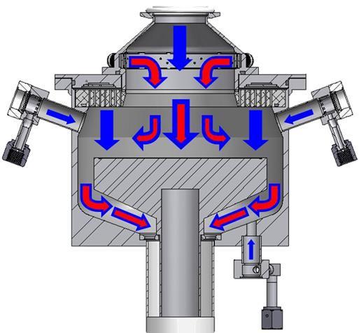
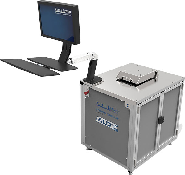
The ALD 150 LX incorporates various reactor design features for advanced, single wafer R&D including remote plasma, real time ellipsometry, and cluster tool integration capabilities. These enhanced features present design challenges that must be overcome to optimize performance, and to minimize reactor downtime. In particular, the additional ports necessary to incorporate these features result in a more complex reactor geometry as well as increased internal volume that make precursor delivery, and effective purging between precursor dose steps, more difficult. Film deposition on internal surfaces (especially inside of reactor ports) should be minimized to avoid excessive precursor waste and buildup of material resulting in premature delamination and particulate formation that require maintenance. On some reactor surfaces deposition must be prevented altogether. For example, conductive layers must be avoided on the transparent windows necessary for light transmission during ellipsometry...
Mina Shahmohammadi from the research group of Professor Christos G. Takoudis, Full Professor in the Departments of Bioengineering and Chemical Engineering at the University of Illinois at Chicago, in collaboration with College of Dentistry, University of Illinois at Chicago, and Kurt J. Lesker Company recently developed conformal atomic layer deposition (ALD) based titanium (IV) oxide (TiO2) thin film processes on Polymethyl Methacrylate (PMMA) displaying excellent surface and mechanical properties for potential engineering, medical, and biomedical applications. The findings were recently published in the Journal of Materials Science...
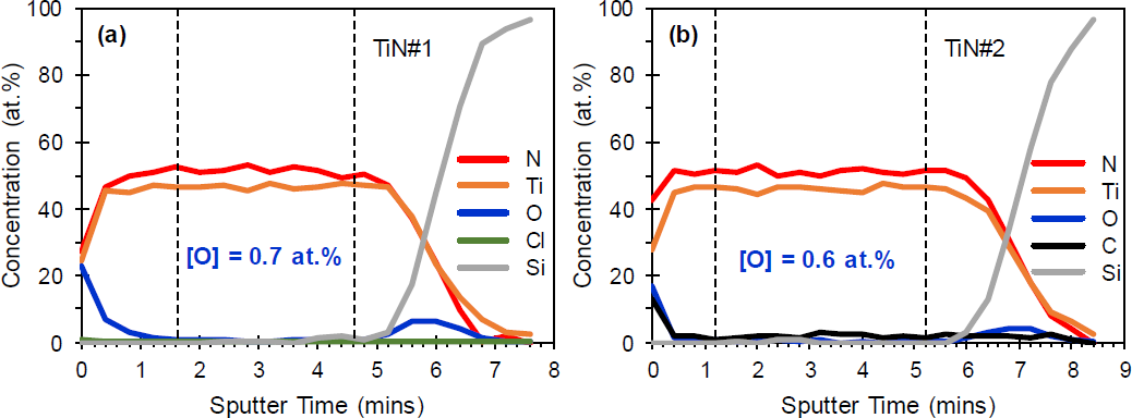
Ultra-high purity (UHP) reactor conditions provide a process environment for growth of nitride thin films with low oxygen content by plasma-enhanced atomic layer deposition (PEALD). In particular, UHP conditions correspond to partial pressures below 10-8 Torr for impurities within the PEALD process environment to limit incorporation before, during and after film growth. In this article we..
This article may be downloaded for personal use only. Any other use requires prior permission of the author and AIP Publishing. This article appeared in Journal of Vacuum Science & Technology A 38, 062408 (2020), and may be found at https://doi.org/10.1116/6.0000454
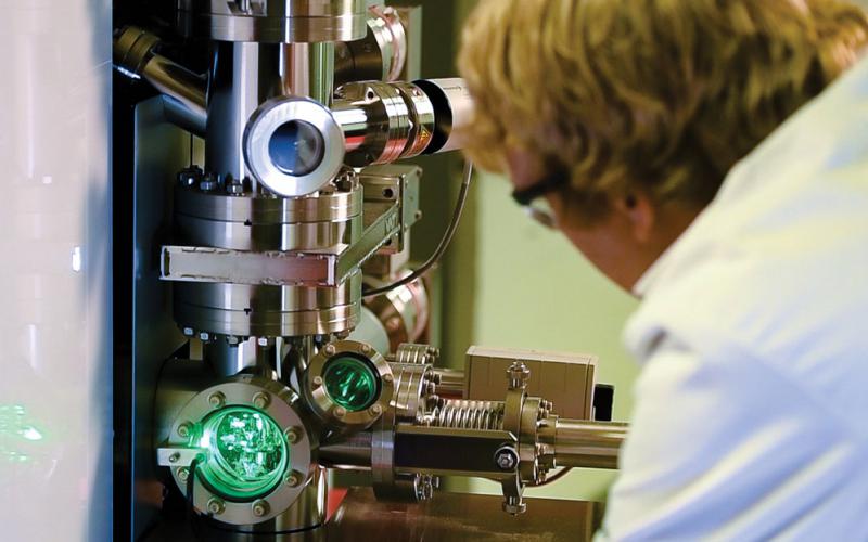
Nanotechnology continues its march through the field of electronics, enabling faster and more energy-efficient computer processors, larger computer memory density and increased battery capacity. These ever-shrinking micro and nanodevices require advanced manufacturing methods to produce. Atomic-scale processing refers to a collection of these methods that may be used to deposit and remove material at the smallest scales, a single atomic layer at a time..
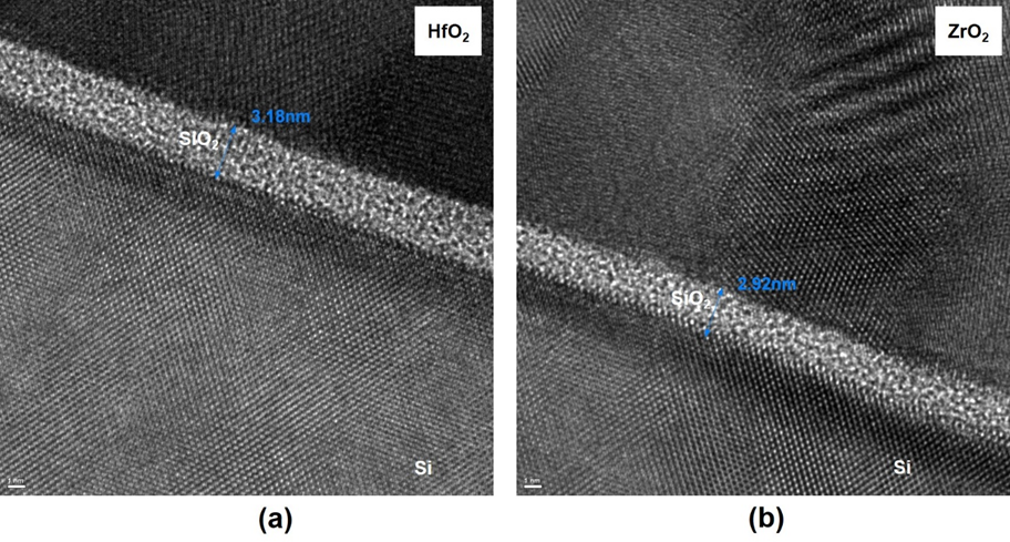
Dr. Zhigang Xiao, Professor of Electrical Engineering at Alabama A&M University, in collaboration with the ALD group in the Kurt J. Lesker Company recently developed the plasma-enhanced atomic layer deposition process and grow high dielectric constant (K) oxide for the application of electronic materials. They grew nanoscale hafnium dioxide (HfO2) and zirconium dioxide (ZrO2) thin films using remote plasma-enhanced atomic layer deposition (PE-ALD) and fabricated complementary metal-oxide semiconductor (CMOS) integrated circuits using the HfO2 and ZrO2 thin films as the gate oxide. Miniaturization in modern semiconductor industry requires thin film deposition to have atomic level control and the deposited film to be conformal and pinhole-free..
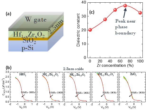
Dr. Kai Ni from the research group of Professor Suman Datta, Stinson Professor of Nanotechnology at the University of Notre Dame, in collaboration with Purdue University and Kurt J. Lesker Company recently developed conformal atomic layer deposition (ALD) based hafnium zirconium oxide thin film processes displaying excellent electrical properties for potential gate oxide complement or replacement in scaled logic and memory technology nodes..
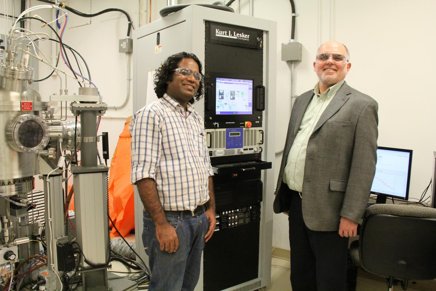
(Edmonton) In the world of nano-scale technology, where work is conducted at the atomic level, even the smallest changes can have an enormous impact. And a new discovery by a University of Alberta materials engineering researchers has caught the attention of electronics industry leaders looking for more efficient manufacturing processes..
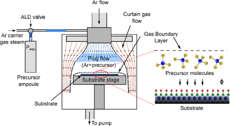
Dr. Nicholas A. Strnad (General Technical Services, LLC) in collaboration with the U.S. Army Combat Capabilities Command Army Research Laboratory and the University of Maryland, College Park have recently developed conformal processes for a variety of lead-based electronic materials with outstanding properties using atomic layer deposition (ALD). The findings have been recently published in the Journal of Vacuum Sciences and Techology, A (ref. 1) and the Digital Repository at the University of Maryland (DRUM) (ref. 2)..
Ready to Advance Your Research?
Do you have any questions? Click below to get in contact with one of our many experienced team members.